
In recent years, EPA has learned a great deal about the extent to which products manufactured to contain PCBs (e.g., paint and caulk) were used in many buildings, including schools, before the manufacture of PCBs was banned by the Toxic Substances Control Act (TSCA). As more buildings were discovered to have PCB contamination, it was also discovered that sometimes PCBs leach from those PCB manufactured products into attached porous building materials. EPA has received many requests to address difficulties the regulated community faces when disposing of this waste properly. In February 2012, EPA issued a proposed reinterpretation to address these concerns and to further protect public health and the environment.
Current Regulations
The Toxic Substances Control Act (TSCA) regulations at 40 CPR 761 provide disposal and cleanup requirements for PCBs. The disposal and cleanup requirements for PCB-contaminated building material depend on whether the material is classified as a PCB bulk product waste (40 CFR 761.62) or PCB remediation waste (40 CFR 761.61).
PCB remediation waste must be cleaned up down to a concentration of 1 parts per million (ppm) for an unrestricted use and if the concentrations of PCBs in the remediation waste are greater than 50 ppm, the remediation waste must be disposed in a TSCA-permitted facility. However, PCB bulk product waste, even at concentrations of PCBs greater than 50 ppm, can be disposed in a non-hazardous solid waste facility, as long as this disposal is permitted by that state’s solid waste regulations.
Since TSCA authority has not been delegated to any of the states, both EPA and state regulations apply. Knowing your specific federal and state requirements for PCB management is essential if you want to remain in compliance with applicable federal and state regulations.
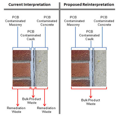
PCB Bulk Product v. Remediation Waste
PCB remediation waste is waste containing PCBs as a result of a spill or release (date and concentration limits apply), e.g., PCB-contaminated soil, sediments, and concrete. PCB bulk product waste is waste derived from products manufactured to contain PCBs in a non-liquid state at 50 ppm or greater. Typical examples are caulk, paint, and sealants.
- PCB-containing caulk, for example, is considered PCB bulk product waste if the concentration of PCBs in the caulk is greater than or equal to (>) 50 parts per million (ppm) (or even less by some state standards, such as Connecticut).
- If PCBs have contaminated either the surrounding building materials or adjacent soil, these materials are considered PCB remediation waste.
EPA Reinterpretation
EPA’s reinterpretation ensures that building materials contaminated with PCBs have disposal options that are efficient, safe, and straightforward. For example, the reinterpretation will mean that the disposal options for the masonry are the same as for the attached PCB caulk.
The reinterpretation specifically addresses the definitions of bulk product waste and remediation waste. This distinction is important as it determines the appropriate cleanup requirements and disposal options. The reinterpretation allows building material (i.e., substrate) “coated or serviced” with PCB bulk product waste (e.g., caulk, paint, mastics, sealants) at the time of disposal to be managed as a PCB bulk product waste, even if the PCBs have migrated from the overlying bulk product waste into the substrate. The following diagram highlights these changes to the definitions.
Resources:
- The final EPA reinterpretation memorandum regarding PCB contaminated building materials: PCB Bulk Product Waste Reinterpretation (October 24, 2012)
- Federal Register Notice – PCBs Bulk Product v. Remediation Waste (February 29, 2012)
The Bottom Line:
EPA’s reinterpretation allows PCB remediation waste adjacent to bulk product waste to be managed as PCB bulk products. The disposal of PCB bulk product wasteis regulated under 40 CFR 761.62 of TSCA. Under this provision, PCB bulk product wastemust be disposed of in one of two ways: disposal in a permitted solid waste landfill or via a risk-based disposal approval process. For situations where PCB caulk, paint, etc. remain attached to building materials, this reinterpretation allows for more efficient removal and disposal.
In order to dispose of PCB bulk product waste in a state-permitted municipal landfill or non-municipal non-hazardous waste landfill, there may be additional sampling, recordkeeping and performance requirements that must be satisfied. Be sure to review 40 CFR 761.62 for specific requirements.
In addition, the remediation waste may be managed as bulk product waste only if it is attached to the contaminated abutting material at the time the material is designated for disposal. If the caulk or paint has been removed from the building material, the substrate would be considered a PCB remediation waste subject to strict management and disposal requirements at concentrations down to 1 ppm.
Please leave a comment or send me an e-mail and tell me what PCB management challenges you are facing and/or other environmental topics that are important to you.

Nancy W. Teolis, J.D., has been a Legal Editor for BLR’s environmental law publications since 1993, focusing primarily on underground storage tanks, pesticides, and hazardous waste-related requirements. Before joining BLR, she worked for the law firm Rudman & Winchell in Bangor, Maine, with an emphasis on asbestos exposure litigation. She received her law degree from Western New England University School of Law in Springfield, Massachusetts, and is a member of the Connecticut bar.
One simple rule. Clean-up what is dangerous for the environment and the people.